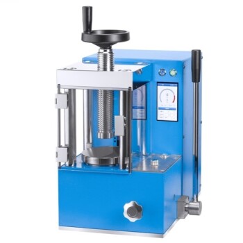
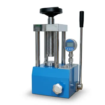
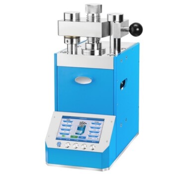
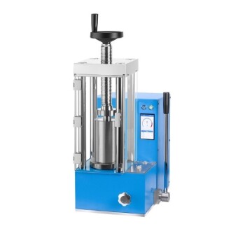
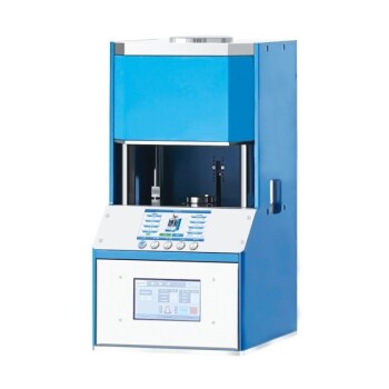
High-precision laboratory presses act as the critical bridge between theoretical design and physical reality in nanoelectronics. They are employed to manufacture dense substrates and pellets using novel semiconductor materials. This process ensures that the physical samples available for testing align perfectly with the high-fidelity simulations created by high-performance computing clusters.
The core value of these presses lies in validation: by strictly controlling the compaction process, researchers ensure physical prototypes accurately reflect digital models, allowing them to solve critical heat and power challenges before mass production begins.
Bridging Simulation and Reality
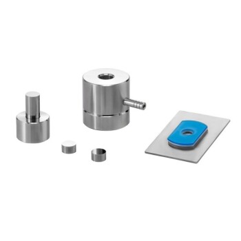
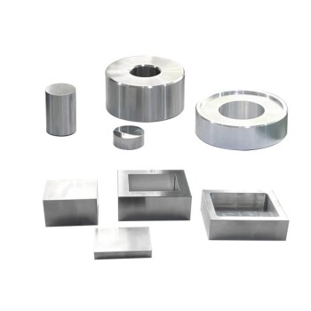
Creating High-Density Substrates
To test new concepts in nanoelectronics, researchers must work with novel semiconductor materials.
High-precision presses are used to compress these raw materials into dense substrates and pellets. This step is foundational, creating the physical canvas upon which electrical properties are tested.
Matching Computational Models
Modern chip design relies heavily on high-fidelity simulations generated by computing clusters.
However, a simulation is only useful if the physical prototype matches the digital parameters. Laboratory presses provide the exact control needed to ensure the manufactured sample is a faithful representation of the computer model.
Solving Physical Constraints
Tackling Heat Dissipation
One of the primary barriers in next-generation chip design is thermal management.
By producing consistent, high-quality samples, researchers can accurately test how new materials handle heat. This allows for the identification of thermal bottlenecks early in the development cycle.
optimizing Power Consumption
Reducing energy usage is a non-negotiable requirement for modern electronics.
Prototypes created via high-precision pressing allow for rigorous testing of electrical characteristics. This verifies that the material offers the power efficiency predicted by the simulations.
Understanding the Trade-offs
Prototyping vs. Production Speed
While these presses offer exceptional control, they are designed for low-volume precision, not high-volume throughput.
The time required to prepare individual pellets or substrates is significantly higher than standard manufacturing processes. This makes them ideal for R&D but unsuitable for mass fabrication.
Scope of Testing
These presses validate the material properties, not necessarily the full circuit architecture.
A successful test on a pressed pellet confirms the semiconductor's potential but does not guarantee the manufacturability of a complex, multi-layered chip. It is a material validation step, not a final product test.
Advancing from Lab to Production
Using high-precision presses allows you to validate the fundamental physics of your design before committing to expensive manufacturing cycles.
- If your primary focus is Material Science: Use these presses to verify that the physical density and structural integrity of your novel semiconductor match your theoretical models.
- If your primary focus is Electrical Engineering: Rely on the samples produced to rigorously test heat dissipation and power consumption data against your simulation results.
By ensuring your physical prototypes mirror your digital simulations, you effectively de-risk the transition to large-scale production.
Summary Table:
| Feature | Significance in Nanoelectronics |
|---|---|
| Substrate Density | Ensures consistent physical properties for novel semiconductor testing. |
| Model Alignment | Matches physical prototypes to high-fidelity computational simulations. |
| Thermal Testing | Enables accurate identification of heat dissipation bottlenecks. |
| Power Validation | Verifies electrical efficiency and material power consumption data. |
| De-risking | Validates fundamental physics before expensive mass production. |
Elevate Your Nanoelectronics Research with KINTEK
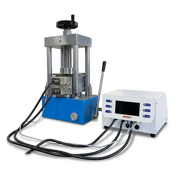
Precision is the foundation of innovation. KINTEK specializes in comprehensive laboratory pressing solutions, offering manual, automatic, heated, multifunctional, and glovebox-compatible models, as well as cold and warm isostatic presses.
Whether you are refining battery research or prototyping next-generation semiconductors, our high-precision presses ensure your physical materials meet the rigorous demands of your digital models. Contact us today to find the perfect pressing solution for your lab and bridge the gap from simulation to reality.
References
- Gautam V. Soni, S. K. Jaiswal. AI-Driven Nanotechnology: Transforming Materials Science, Medicine, and Electronics. DOI: 10.55041/ijsrem52212
This article is also based on technical information from Kintek Press Knowledge Base .
Related Products
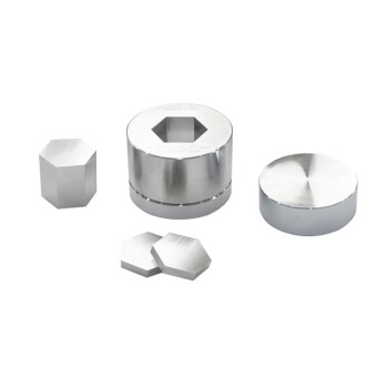
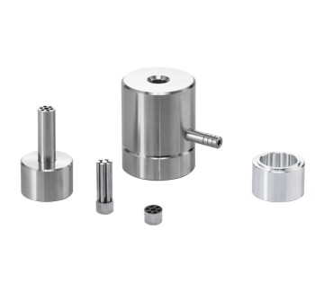
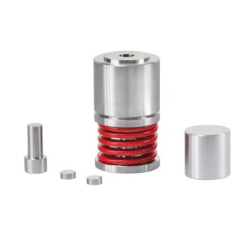
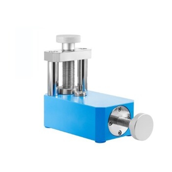
- Lab Polygon Press Mold
- Special Shape Lab Press Mold for Laboratory Applications
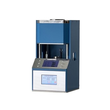
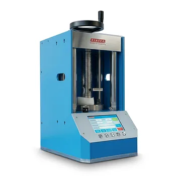
- Automatic High Temperature Heated Hydraulic Press Machine with Heated Plates for Lab
- 24T 30T 60T Heated Hydraulic Lab Press Machine with Hot Plates for Laboratory
- Lab Round Bidirectional Press Mold
People Also Ask
- What is the significance of standardized molds in lab presses? Ensure Precise Seal Material Evaluation
- What role do precision positioning and pressure molds play in single-lap joints? Ensure 100% Data Integrity
- Why is precise cooling management of the lab press mold necessary? Protect Core Integrity in Thermoforming
- How does the geometry of laboratory molds influence mycelium-based composites? Optimize Density and Strength
- What is the purpose of incorporating cartridge heaters into a lab press mold for MLCC block compression? Optimize Results