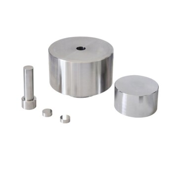
Hot press mounting with conductive epoxy resin is required to establish a reliable electrical connection between your Hafnium Nitride (HfN) sample and the microscope stage. Without this conductive path, the electron beam used in Scanning Electron Microscopy (SEM) will cause electrons to accumulate on the surface of the ceramic material, leading to significant imaging artifacts.
Creating a continuous conductive path is the only way to effectively drain excess electrons from the HfN surface. This prevention of charge buildup is strictly necessary for Electron Backscatter Diffraction (EBSD), where signal stability is required to generate accurate grain orientation maps and high-quality microstructural images.
The Physics of Surface Charging
The Problem with Ceramics in SEM
Hafnium Nitride is a ceramic material. Like many ceramics, it is prone to accumulating electrical charge when bombarded by the high-energy electron beam of an SEM.
If these electrons have nowhere to go, they build up on the sample surface. This phenomenon, known as charging, creates an electrostatic field that deflects the incoming electron beam.
The Role of Conductive Epoxy
Conductive epoxy resin acts as an electrical bridge. By embedding the sample in a medium that contains conductive fillers (often carbon or copper), you create a direct path to the ground.
This allows the excess electrons deposited by the beam to flow harmlessly away from the HfN surface and into the microscope stage. This flow effectively neutralizes the surface potential, stabilizing the sample for analysis.
Critical Implications for EBSD Analysis
Demanding Signal Requirements
The primary reference highlights that this mounting method is particularly vital for Electron Backscatter Diffraction (EBSD). EBSD is far more sensitive to surface conditions than standard topographic imaging.
Because EBSD relies on analyzing diffraction patterns generated from the top few nanometers of the surface, any electrostatic interference will degrade the pattern quality.
Achieving High-Quality Mapping
To acquire accurate grain orientation maps, the electron beam must scan across the sample with high precision. Charging causes "drift," where the beam is repelled from its intended path.
Conductive hot press mounting ensures the beam stays positioned correctly. This stability allows for the acquisition of sharp, distortion-free microstructural images and reliable crystallographic data.
Understanding the Trade-offs
Mechanical Stress Factors
While hot press mounting provides excellent edge retention and conductivity, it involves subjecting the sample to both heat and significant pressure.
You must ensure your specific HfN sample is structurally sound enough to withstand the compression of the mounting press without cracking or altering its microstructure.
Preparation Time vs. Data Quality
This method is more time-intensive than using cold-mounting resins or simple conductive tape. It requires specialized equipment (a mounting press) and a heating cycle.
However, for EBSD on ceramics, the trade-off is non-negotiable: the time invested in preparation is the only way to guarantee usable data.
Making the Right Choice for Your Goal
To ensure you are applying this technique correctly for your specific needs:
- If your primary focus is EBSD Analysis: You must use hot press mounting with conductive epoxy to prevent drift and ensure clear diffraction patterns.
- If your primary focus is Quick Topographic Imaging: You might get by with conductive tape, but recognize that image quality will suffer due to potential charging.
Proper grounding during sample preparation is the single most important factor in transforming a noisy, distorted scan into a high-fidelity microstructural map.
Summary Table:
| Feature | Hot Press with Conductive Resin | Alternative Methods (e.g., Tape) |
|---|---|---|
| Electrical Conductivity | Excellent (Continuous path to ground) | Limited (Surface path only) |
| SEM Imaging Quality | High (No charging artifacts) | Low (Prone to drift and noise) |
| EBSD Suitability | Essential for accurate mapping | Not recommended due to signal degradation |
| Edge Retention | Superior | Poor |
| Process Requirements | Heat and Pressure applied | Room temperature/Simple application |
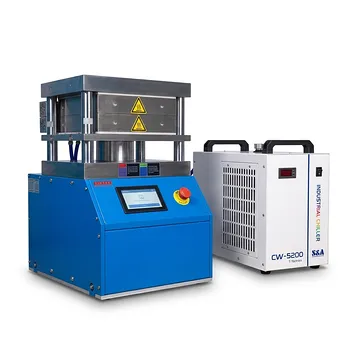
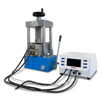
Precision sample preparation is the foundation of reliable battery research and material analysis. KINTEK specializes in comprehensive laboratory pressing solutions, offering a full range of manual, automatic, heated, and multifunctional models, as well as cold and warm isostatic presses. Whether you are mounting ceramic HfN for EBSD or developing next-generation electrodes, our equipment ensures the structural integrity and conductivity your research demands. Contact us today to discover how KINTEK's pressing technology can enhance your lab's data accuracy and efficiency!
References
- Katherine Vinson, Gregory B. Thompson. Plasticity mechanisms in HfN at elevated and room temperature. DOI: 10.1038/srep34571
This article is also based on technical information from Kintek Press Knowledge Base .
Related Products
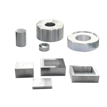
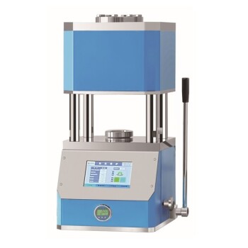
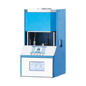
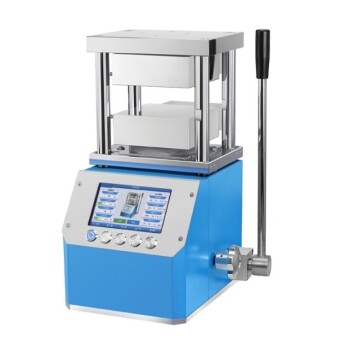
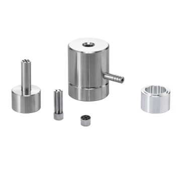
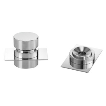
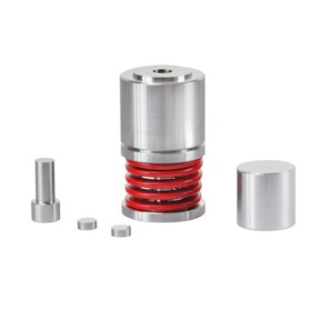
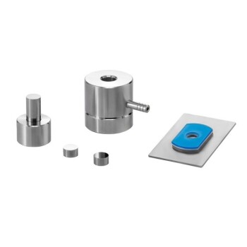
- Lab Heat Press Special Mold
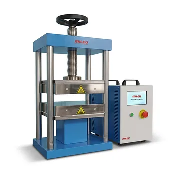
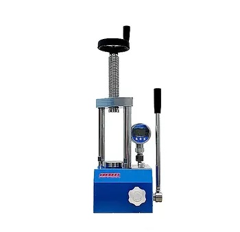
- Automatic Heated Hydraulic Press Machine with Hot Plates for Laboratory
- Automatic High Temperature Heated Hydraulic Press Machine with Heated Plates for Lab
- 24T 30T 60T Heated Hydraulic Lab Press Machine with Hot Plates for Laboratory
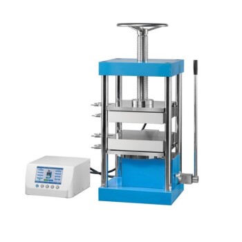
- Warm Isostatic Press for Solid State Battery Research Warm Isostatic Press
People Also Ask
- How is a laboratory heat press utilized in MEA preparation? Achieve High-Efficiency Iron-Chromium Redox Flow Batteries
- Why is a laboratory heated press typically required when researching the mechanical properties of polyrotaxane materials?
- What critical process conditions does a laboratory heated lab press provide? Optimize AEM Electrolyzer Assembly
- What is the purpose of incorporating cartridge heaters into a lab press mold for MLCC block compression? Optimize Results
- Why is a laboratory heat press necessary for biodegradable films? Unlock Precision Bonding and Barrier Performance