The primary purpose of grinding AgSb0.94Cd0.06Te2 ingots is to drastically increase the specific surface area of the inorganic phase by reducing the bulk material into fine powders. This physical transformation is a prerequisite for achieving a uniform mixture with the polymer matrix, which directly dictates the structural integrity and electrical performance of the final film.
Grinding is not merely a size-reduction step; it is a critical interface engineering process. By maximizing surface area, it enables homogeneous mixing with the polymer dispersion, ensuring the final material exhibits the consistent microstructure necessary for optimized charge transport.
The Mechanics of Microstructural Optimization
Increasing Specific Surface Area
The grinding process—whether manual or mechanical—converts large ingots into fine particles ranging from 0.25 to 20 micrometers.
This significant reduction in size exponentially increases the specific surface area. A larger surface area allows for more extensive physical contact between the inorganic AgSb0.94Cd0.06Te2 and the surrounding medium.
Facilitating Uniform Dispersion
The target application involves mixing these powders with PEDOT:PSS dispersions to create a slurry.
Fine particles are essential for this step because they can be distributed evenly throughout the liquid dispersion. Large chunks or irregular fragments would resist integration, leading to a clumpy, non-uniform mixture that is unsuitable for coating applications.
Impact on Final Film Performance
Ensuring Microstructural Consistency
The quality of the slurry directly determines the quality of the resulting film formed during the coating process.
By starting with a uniformly mixed slurry, the final solid film retains high microstructural consistency. This means the inorganic and organic phases are blended homogeneously, without phase separation or distinct defects caused by large particles.
Optimizing Charge Transport
The ultimate engineering goal of this process is to improve the material's electrical properties.
A consistent microstructure minimizes interruptions in the material's conductive network. This continuity optimizes charge transport paths, allowing electrons or holes to move more freely through the composite material.
Understanding the Critical Constraints
The Necessity of the Particle Size Range
While grinding is beneficial, the specific target range of 0.25 to 20 micrometers is non-negotiable for success.
This range represents the "sweet spot" for this specific material system. Particles larger than 20 micrometers would likely disrupt the film continuity, creating blockages or voids. Conversely, maintaining this distribution ensures the inorganic phase integrates seamlessly with the PEDOT:PSS chains.
Risks of Poor Processing
If the grinding process is inconsistent, the resulting slurry will fail to achieve homogeneity.
Inconsistent mixing leads to unpredictable film properties. Areas with poor dispersion will exhibit inferior charge transport, rendering the material ineffective for high-performance applications.
Applying This to Material Synthesis
To ensure you are maximizing the potential of your AgSb0.94Cd0.06Te2 composite:
- If your primary focus is Film Quality: Ensure your grinding protocol strictly adheres to the 0.25–20 micrometer range to guarantee a smooth, defect-free coating.
- If your primary focus is Electrical Performance: Prioritize the uniformity of the mixing stage, as the homogeneity of the slurry is the primary driver of optimized charge transport paths.
The success of the final composite relies entirely on the precision of this initial mechanical processing step.
Summary Table:
| Process Objective | Mechanism | Outcome on Film |
|---|---|---|
| Surface Area Increase | Size reduction to 0.25–20 μm | Enhances interface contact between phases |
| Slurry Homogeneity | Uniform dispersion in PEDOT:PSS | Prevents phase separation and structural defects |
| Structural Integrity | Consistent microstructural blending | Ensures smooth, high-quality coating application |
| Electrical Efficiency | Continuous conductive network | Optimizes charge transport and electrical paths |
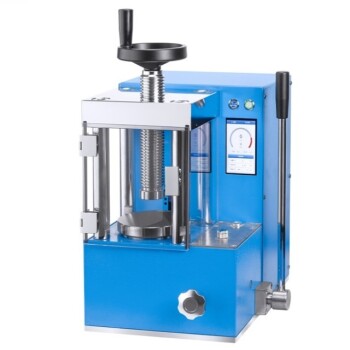
Elevate Your Material Research with KINTEK Precision
Achieving the perfect 0.25–20 μm particle size for your AgSb0.94Cd0.06Te2 ingots is critical for superior film performance. KINTEK specializes in comprehensive laboratory pressing and grinding solutions designed to meet the rigorous demands of battery and semiconductor research.
Our range includes:
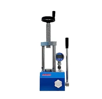
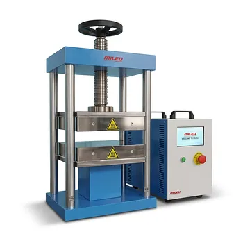
- Manual & Automatic Presses for sample preparation.
- Heated & Multifunctional Models for advanced material synthesis.
- Isostatic Presses (Cold/Warm) for uniform density and structural integrity.
Don't let inconsistent grinding compromise your charge transport. Contact KINTEK today to discover how our specialized equipment can enhance your lab's efficiency and material quality.
References
- Mahima Goel, Mukundan Thelakkat. Highly Efficient and Flexible Thin Film Thermoelectric Materials from Blends of PEDOT:PSS and AgSb<sub>0.94</sub>Cd<sub>0.06</sub>Te<sub>2</sub>. DOI: 10.1002/aelm.202500118
This article is also based on technical information from Kintek Press Knowledge Base .
Related Products
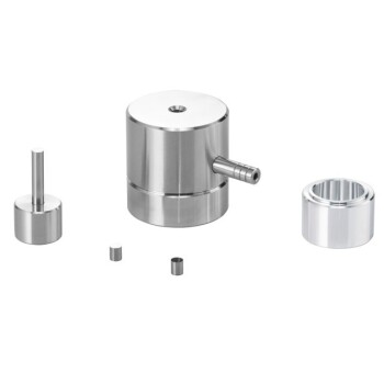
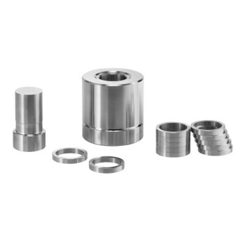
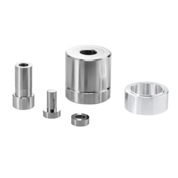
- Lab Cylindrical Press Mold for Laboratory Use
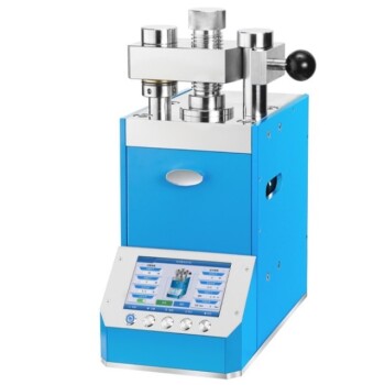
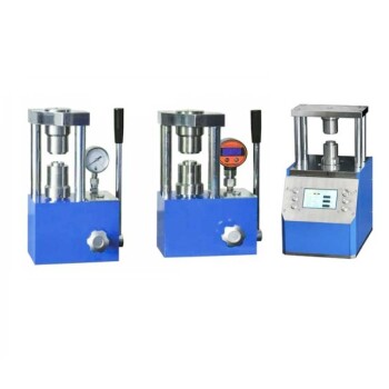
- Automatic High Temperature Heated Hydraulic Press Machine with Heated Plates for Lab
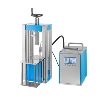
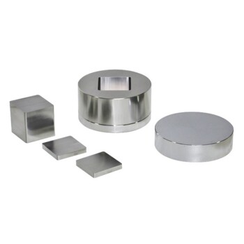
- Laboratory Hydraulic Split Electric Lab Pellet Press
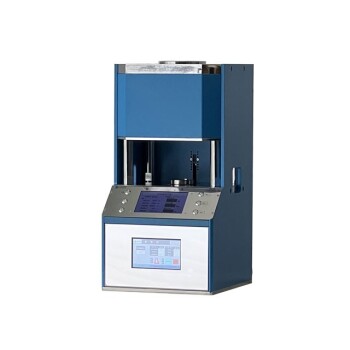
- Automatic Laboratory Hydraulic Press for XRF and KBR Pellet Pressing
- Manual Laboratory Hydraulic Press Lab Pellet Press
People Also Ask
- How does the geometry of laboratory molds influence mycelium-based composites? Optimize Density and Strength
- What role do precision positioning and pressure molds play in single-lap joints? Ensure 100% Data Integrity
- Why is a high-performance laboratory molding press critical for in-situ electrolyte formation? Unlock Battery Success
- What is the function of a pressing tool in thermoplastic panels? Master Precision Shaping & Fusion Bonding
- Why is precise cooling management of the lab press mold necessary? Protect Core Integrity in Thermoforming